A dopant added into the base material lies at the heart of semiconductor technology. For example, not just germanium but germanium with selenium or some other element. The dopant makes it easier for electrons to move from the valence band of the base material into its conduction band as well as into the additive conduction band. Thus, a great number of “holes” are formed in the valence band. By adding various dopants conduction types can be regulated. As a result, semiconductors of a p-type or electronic semiconductors capable to improve the conduction are produced. In this way it is possible to set new properties of the substance, to construct semiconductor materials with various characteristics to be in need by scientists or in industries. The main difficulty is to develop the better ways of adding dopants into the base material.
For this purpose different methods were used. Being given the required energy the dopant was first ionized and embedded deep in the semiconductor. One of the other methods consisted in laser doping. Both of the methods had their weak points.
A group of researchers, with V.V. Rykov at the head, offered another technique. They worked on germanium containing a small selenium admixture. And the base material was doped with nickel or aluminum. Technically, the whole doping process included covering semiconductor substrates with very thin translucent metallic film. Then the substrates were exposed to the strong magnetic field effect and light irradiation. By means of power modes used in this process heating of the conductor surface layer at the ligature contact area was eliminated. Thus, mechanical stresses of other methods were reduced. This led to the improvement of doped layer characteristics.
Developed by V.V. Rykov and his team, the method was patented. V. Rykov also studied and did holography. It is not a new scientific and practical sphere. The development of laser made it easier for stereoscopic pictures recorded by a special method on photosensitive media to be widely used in technology and everyday life. It became possible to apply holograms in documents, visit cards and logotypes – for the purpose of protection against counterfeiting
V. Rykov developed a new method of applying holograms on new materials. He offered halcohenide amorphous semiconductors for this process instead of gelatin and other photosensitive media used before. Pictures from the new semiconductors were easier copied on metal and then on polymeric materials or paper. The method of recording the picture was also improved. The process of capturing the original image was repeated many times from several positions taking various angles. This joint work was made by V.V. Rykov with Saint Petersburg State Optical University. The VSU Chemical school students took an active part in the study.
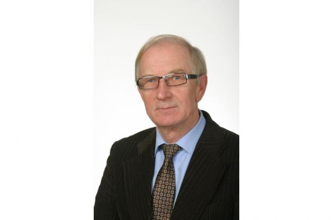
Reference: V.V. Rykov, Candidate of Physical and Mathematical Sciences, associate Professor. He started to work at Inorganic Chemistry Faculty as a senior laboratory assistant, defended a Candidate’s dissertation in the University of St. Petersburg, and was offered a position of an associate Professor at the Faculty of Industrial Electronics. He also held positions of the Trade Union Committee Chairman of Vyatka State University, the Secretary of the University Scientific Council and Kirov Rector’s Council, the Vice-Rector for Evening and Correspondence Training, the Vice-Rector for Studies. He is an author of more than 70 publications on solid-state physics, several certificates of authorship and patents.\
From the book VyatSU: biography, 1998